
News
Direct answer: SPI, AOI and X-ray inspect the board. None of them proves the circuit works. Three electrical and functional methods do that job, and they catch different faults. ICT measures every component and connection through a bed-of-nails fixture — fast, but it needs test points and a fixture built for that board. Flying probe makes the same kind of measurements with moving probes and no fixture — flexible, but slower per board. Functional test powers the board up and checks that it does its job — the only one of the three that can catch a firmware or timing fault, and the only one that cannot tell you which component failed. Choose by volume, design stability and how often the board changes, not by which brochure is loudest. JHIMS does not sell ICT, flying-probe or functional-test equipment — this is a test-method guide, not a product guide.
By the time a board reaches the end of an SMT line, it has usually passed three inspection gates. SPI measured the solder paste before any part was placed. AOI checked placement and visible solder joints after reflow. X-ray looked at the joints nobody can see, under BGAs and QFNs. Each gate proved something real — and each gate is blind to a different class of fault.
None of the three applies power to the board. None of them measures the value of a single component. A 10 kΩ resistor looks exactly like a 100 kΩ resistor. A solder joint can look wetted on the outside and be open underneath the part. A board can be perfectly placed, perfectly soldered, and still not boot — because the wrong firmware was loaded, or a power rail collapses under load, or two nets are shorted where no camera can see.
That is the gap electrical and functional test close. Optical inspection answers, “Does the board look right?” Electrical test answers, “Is it connected right, with the right parts?” Functional test answers, “Does it do its job?” A line that stops at the optical gates is shipping boards that look right. Whether they work is still untested.
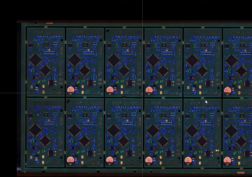
Figure 1: A populated panel as the AOI camera sees it — every part present and placed. This view can confirm placement. It cannot confirm that the circuit works. Frame from the official JHIMS JUTZE AOI teaching video, cropped to the camera image.
The rest of this guide follows the inspection chain to its end: the SPI-or-AOI buy-order decision covers the first two gates, and the X-ray guide covers hidden joints. This article starts where all three stop.
Electrical test proves three things, and it is worth keeping them separate, because each method below proves a different subset.
First, connectivity: every net is connected as designed — no opens, no shorts. Second, component correctness: the parts are present, the right way round, and the right value — resistance, capacitance, inductance, diode and transistor junctions. Third, behaviour: when powered, the board does what its specification says — boots, talks on its interfaces, holds its power rails under load.
Optical inspection proves none of these directly. It infers them from appearance: a part in the right place is probably the right part; a joint that looks wetted is probably connected. “Probably” is the problem. The table below lists the fault families that routinely pass optical inspection and shows which test catches each one.
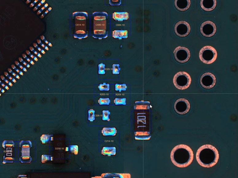
Figure 2: An AOI camera close-up — solder joints and component placement, with the inspection program’s part windows. A joint can look right here and still fail an electrical test. Frame from the official JHIMS JUTZE AOI teaching video, cropped to the camera image.
| Fault that optical inspection can miss | What catches it |
|---|---|
| Wrong component value (10 kΩ fitted where 100 kΩ belongs) | ICT or flying probe — they measure the value |
| Open or short under a component body | ICT or flying probe; X-ray only shows the joint, not the connection |
| Reversed polarity where the marking is hidden | ICT or flying probe — diode and junction checks |
| Missing part under a shield or connector | ICT or flying probe — the net measures open |
| Wrong or missing firmware | Functional test only |
| Power rail that collapses under load, timing fault | Functional test only |
| Marginal joint that conducts today and fails after vibration or thermal cycling | None of the three reliably — this is a workmanship and reliability question, not a test-coverage question |
Two cautions belong here, before the methods. First, no test method has a fixed coverage percentage. How much of a board any electrical test can verify depends on how many nets it can reach — test points, accessible pads, component leads — and that is decided in the layout, not at the test station. Any article that prints a single coverage figure as a standard is asking to be misapplied. Second, there is no universal “acceptable defect rate” for a board. What is acceptable depends on the product, the customer and the contract. This guide gives you a decision method, not a number to copy.
In-circuit test presses the assembled board onto a fixture carrying a spring-loaded pin for every test point — the “bed of nails.” All test points are contacted at once, and the tester works through the board in stages: unpowered checks for shorts and opens first, then passive component values and simple semiconductor junctions, then powered checks for more complex devices.
What it catches. Opens, shorts, wrong or missing component values, reversed polarity, and a range of IC faults — and it locates the fault to a specific net or component. That location is worth more than it sounds: when a board fails, the operator knows where to look instead of starting a manual hunt. For diagnosis and rework speed, ICT is the strongest of the three methods.
What it needs. Three things, all decided before the board is built. Dedicated test pads on the layout, on the nets that matter — without access, there is nothing to measure. A fixture designed and built for that board, plus a test program. And a stable design: when the layout changes, the fixture may need rework or replacement.
What it misses. Anything that only appears when the circuit runs — firmware behaviour, timing, interface protocol, power behaviour under load. ICT tests components and connections. It does not test the product.
Where it fits. Stable designs, repeat orders, medium to high volume. Because every point is contacted at once, a board is typically measured in seconds, and the per-board cost after the fixture exists is low. The fixture itself is a one-off cost that takes weeks to design and build — which is exactly why the volume question matters, and why Section 7 starts there.
A flying-probe tester makes the same kind of electrical measurements as ICT, using a small number of motor-controlled probes that travel to test points under program control — usually a handful of probes, working on both sides of the board. There is no fixture built for the board. The probes contact pads, vias and component ends directly, following the test program.
What it catches. The same electrical fault classes as ICT: opens, shorts, passive values, orientation errors — within the reach of its probes. For a prototype or a first build, that is usually the whole question.
What it costs you. Time per board. The probes visit points one at a time, so the same board takes minutes rather than seconds. The number of probes is small, so the number of points tested in one pass is limited by the program and the time available. And like ICT, it is mostly a DC and low-frequency measurement: it proves connections and values, not high-speed behaviour.
Where it fits. Prototypes, new-product introduction, low-volume and high-mix production, and any board whose design is still moving. With no fixture to design, build, store or rework, the cost of adding another product to the test roster is small — a program change, not a hardware change. That is the whole trade: no fixture cost and no fixture lead time, paid for in slower per-board testing.
A common pattern is to use both methods across a product’s life: flying probe while the design is changing and volumes are small, ICT once the design is stable and the volume justifies the fixture. Neither choice is permanent, and the switch is a normal production decision, not a sign the first choice was wrong.
Functional test powers the assembled board and exercises it the way the end product will: inputs applied, outputs measured, interfaces checked, firmware run, power rails watched under load. It is the closest proxy to real use, and the only method in this guide that can answer the question the customer actually asks — does the board work?
What it catches. Faults that only appear in operation: wrong firmware, a board that does not boot, timing problems, interface failures, power sequencing errors, a sensor input that reads wrong. None of the other methods can see these, because none of them runs the board.
What it misses. Two classes deserve emphasis. First, marginal joints: a joint that conducts today can pass a functional test and fail later, after vibration or thermal cycling. Functional test proves the board works now, not that it will keep working. Second, protection components that never act in normal operation — a protection diode that has failed open will not show up in a test that never triggers it. And when a functional test fails, it reports that a function failed, not which component caused it. Finding the cause usually needs an experienced engineer and more time than an ICT failure report takes.
What it needs. A test plan or procedure that defines what “works” means for this board, the firmware to run, and usually a test stand that emulates the board’s environment — mating connectors, loads, sometimes another board alongside. Developing that plan and stand is often the most expensive part of functional test, even though the hardware itself is simple. A functional test without a written plan is an opinion, not a test.
Where it fits. On top of an electrical test, not instead of one. A board that passes functional test with a marginal joint or an untested protection component is a board that passed the wrong test for those faults. The normal stack is: optical inspection, then electrical test (ICT or flying probe), then functional test. Each layer catches what the previous layer cannot.
| Method | What it proves | What it misses | What it needs from you | Best when |
|---|---|---|---|---|
| ICT (bed of nails) | Opens, shorts, component values, polarity; fault located to a net or part | Firmware, timing, behaviour under load; nets with no test access | Test points in the layout; a fixture and program per board design | Stable design, repeat orders, medium to high volume |
| Flying probe | Same electrical fault classes as ICT, within probe reach | Firmware, timing, behaviour under load; limited by probe count and time | Accessible pads or test points; a test program | Prototypes, NPI, low volume, high mix, changing designs |
| Functional test | The board does its job: boot, firmware, interfaces, power under load | Marginal joints; protection parts that never act; which component failed | A written test plan, firmware, usually a test stand | As the last gate, on top of an electrical test |
One more method is worth naming so it is not confused with these three. Boundary scan (JTAG) tests connections through the pins of JTAG-capable parts, without probes — but only on boards designed for it, and only for the nets the boundary-scan chain reaches. It is a fourth option for boards that carry it, and outside this guide’s scope.
The economics can be stated in one paragraph, without a single price. A fixture is a fixed cost per board design: spread over many boards, it becomes small per board; spread over a few hundred, it dominates the cost of testing. A flying probe has almost no setup cost per design, but each board takes longer to test, so its cost per board stays roughly flat as volume grows. That is the whole trade, and it is why the right answer flips with volume.
| Your situation | Start with | Why |
|---|---|---|
| Prototypes and first builds, design still changing | Flying probe + functional test | No fixture to scrap when the layout changes; functional test proves the design itself works |
| Low volume, many different products | Flying probe + functional test | One tester covers the whole mix with program changes only |
| Stable design, repeat orders, throughput pressure | ICT + functional test | Fixture cost spreads over volume; seconds per board keeps the line moving |
| Customer contract requires per-board electrical evidence | ICT or flying probe on every board | Only an electrical test produces per-board, per-net evidence; functional test alone does not |
| Board must prove it works as a product, not just as a circuit | Functional test, added to the electrical test above | Only a powered test proves behaviour; add it, do not substitute it |
Before ordering anything, answer four questions in writing. First, how many boards per year for this design, and how often does the design change? Second, does the layout have test points on the nets that matter — and if not, who pays to add them? Third, what does the customer contract require: per-board electrical evidence, functional evidence, or both? Fourth, who writes the test program and the functional test plan, and who owns them when the design changes? A test method chosen without these answers is a purchase, not a decision.
One question comes up on every line: must every board go through every test? Many lines run an electrical test on every board and functional test on a sample — or functional test on every board for a high-risk product. Whether sampling is acceptable depends on the product’s risk, the failure cost, and what the customer requires. There is no universal sampling rule, and this guide does not invent one. Decide it per product, in writing, with the customer’s requirements in front of you.
Test coverage is decided in the layout, not at the test station. The cheapest time to get it right is before the board is drawn, and the most expensive time is after the first prototypes fail electrical test for lack of access.
Put test points on the nets that matter. Every net whose failure would escape to the customer deserves a reachable point — small, on an accessible side, clear of tall components and keep-out zones. A net with no access cannot be measured, and no test method can recover that afterwards.
Keep the points reachable. Probes and fixture pins need physical access. Points buried under a shield, a connector or a heatsink are points that do not exist. Review access with the test house or EMS before the layout is frozen, not after the first build.
Do not forget the fiducials. Placement accuracy is what the test then verifies: the machine can only place as accurately as it knows where the board is. Fiducial marks are the cheapest accuracy on the line, and a board placed off-target will fail electrical test for a placement reason, not a test reason.
Start the chain at receipt. The wrong part caught at the receiving bench never reaches the test station. Incoming inspection — label, moisture indicator and physical checks — is the first gate in this chain, and it is the cheapest place in the whole factory to catch a wrong reel.
Talk to the test house early. Whoever will test the board — your own line or an EMS partner — should see the layout before it is frozen. The questions are simple: which nets can you reach, which can you not, and what would you change? A one-hour review at layout stage is worth more than a fixture redesign after first articles.
1. Skipping electrical test because AOI passed. AOI proves appearance. A wrong-value part, an open under a component and a short nobody can see all pass AOI. The boards that escape this way are the expensive ones — they fail at the customer, not on the line.
2. Ordering ICT for a board with no test points. A fixture without access is a press that cannot measure. The failure is discovered after the fixture is built, when it is too late to add points cheaply. Check access before ordering, not after.
3. Using functional test as the only test. A board can pass functional test with a marginal joint, a wrong-value part in a tolerant circuit, or a failed protection component. Functional test proves the board works today. It does not prove it is built right.
4. Treating a functional pass as proof the board will last. Marginal joints and early-life failures are reliability questions, not functional questions. Burn-in and stress screening exist for that reason — they are a separate decision from pass/fail testing, and they belong in the reliability plan, not in the test specification.
5. Testing at the end of the line with no rework path. A test that finds failures without a diagnosis and rework loop is a scrap generator. ICT’s net-level fault location is part of its value: it tells the operator where to look. Functional failures need diagnosis time — budget for it, or the test station becomes a bottleneck of unexamined boards.
JHIMS builds the inspection stations that sit before electrical test, not the test equipment itself. To state it plainly: JHIMS does not sell ICT, flying-probe or functional-test equipment, and nothing in this guide should be read as a product recommendation for those methods.
What JHIMS does supply is the optical chain that makes electrical test meaningful — because a board that fails electrical test for a print or placement reason should have been caught earlier, cheaper. The 3D SPI models S460 and S630 measure every paste deposit — volume, area, height, XY offset and shape — with the same core measurement set on both listings: a 5-megapixel telecentric camera, 16 µm resolution, Gage R&R under 10%, 0.45 s per field of view, 150 µm minimum pad spacing, and a 0.4–7 mm board thickness range. Board size is model-specific: the S460 covers up to 460 × 460 mm and the S630 up to 630 × 550 mm. See the JHIMS S630 3D SPI machine and the SPI-or-AOI buy-order guide, which documents the dual-listing cross-check.
On the AOI side, the JHIMS XI-2000 is the post-reflow optical gate. Its own line workflow shows the order this guide follows: printer, SPI, placement, reflow, AOI — and then ICT or functional test. The optical gates prove the board looks right. The electrical and functional tests prove it works. Neither half substitutes for the other.
Limitations, stated plainly: this guide gives you a decision method, not measured payback or coverage figures — both depend on your defect mix, volumes and board access, and no percentage is claimed here. Fixture costs and test times vary too widely between boards and suppliers to quote as facts, so none are printed above; get them quoted against your board. Model-specific figures that appear on only one site listing, and any price or rating figures on product pages, are deliberately not quoted; confirm them with JHIMS before specifying.
Can AOI replace electrical test?
No. AOI inspects appearance after placement. It cannot measure a component’s value, confirm a connection under a part, or prove the board works when powered. A board can pass AOI with a wrong-value part, an open joint under a component, or missing firmware.
Does ICT test firmware?
No. ICT tests components and connections, mostly unpowered. Firmware behaviour, boot, timing and interfaces need a functional test.
Is flying probe enough for production?
For low-volume and high-mix production, yes — that is what it is for. At high volume, the per-board test time becomes the bottleneck, and that is when a fixture-based ICT pays. Many lines use flying probe for prototypes and switch to ICT when the design stabilises.
Does functional test find bad solder joints?
Only if the joint fails while the board is running. A marginal joint can pass functional test today and fail later, after vibration or thermal cycling. Joints are a workmanship and inspection question; functional test is a behaviour question.
What should I ask my EMS or test house before ordering?
Which nets can you reach on this layout, and which can you not? Who owns the fixture, the test program and the functional test plan when the design changes? What does a failure report contain — a net and component, or just pass/fail? And is the functional test plan included in the quote, or priced separately?
Bottom line: Optical inspection proves the board looks right. ICT or flying probe proves it is connected right, with the right parts. Functional test proves it works. Use flying probe while the design is moving and volumes are small, ICT when the design is stable and volume justifies the fixture, and functional test on top of one of them — never instead of one of them. And put the test points in the layout before the board is frozen, because no test method can measure a net it cannot reach.
For SPI specifications, AOI specifications, or a demonstration on your boards, contact JHIMS at [email protected].


 Teams
 whatsapp
 telegram
