


How PCB Depaneling & Laser Engraving Transform 2026 Electronics
As the global printed circuit board (PCB) market surpasses $900 billion in 2026 and AI-driven hardware demand intensifies, one process quietly stands between a flawless electronic device and a costly field failure: depaneling. The method by which individual PCBs are separated from manufacturing panels has evolved from a manual afterthought into a precision engineering discipline. This article examines the three generations of depaneling technology—V-Cut, router, and laser—alongside the rising role of laser engraving for traceability, with quantified insights to help electronics manufacturers navigate the fast-changing landscape.
1. PCB Manufacturing in 2026: Why Cutting Precision Matters More Than Ever
The PCB industry enters 2026 at an inflection point. According to Prismark Partners, global PCB output reached approximately $867 billion in 2025 and is projected to exceed $900 billion in 2026, with a compound annual growth rate (CAGR) of 4.5% through 2029. Crucially, Goldman Sachs revised its AI PCB total addressable market estimate to $266 billion by 2027—representing a staggering 140% CAGR. China alone invested 1,053 billion RMB in PCB manufacturing in 2025 (CINNO Research), with AI computing and automotive electronics serving as the primary growth engines.
This explosive growth exposes persistent manufacturing pain points:
- Stress-induced defects—Manual or crude mechanical depaneling creates micro-cracks in solder joints and components, with studies showing up to 3–5% latent failure rates in high-density boards separated by inadequate methods.
- Precision ceilings—As component pitch shrinks below 0.3mm and board layers exceed 20 in AI servers, traditional depaneling methods struggle to maintain ±0.1mm accuracy without collateral damage.
- Throughput bottlenecks—High-mix, low-volume production lines require rapid changeover between board designs; inflexible depaneling setups can become the production line's slowest link.
- Traceability compliance—IPC-1782 and automotive industry standards increasingly mandate permanent, machine-readable marking on every PCB, adding a new dimension to the cutting and engraving workflow.
- Material diversity—From standard FR4 to aluminum-backed LED substrates, ceramic RF boards, and flexible polyimide circuits—each material demands a tailored depaneling approach, complicating equipment selection.
2. Three Generations of PCB Depaneling Technology
2.1 V-Cut Depaneling — The Proven Workhorse
V-Cut (V-Scoring) depaneling remains the most widely deployed separation method in 2026. The process involves pre-cutting V-shaped grooves at designated panel positions during PCB fabrication, which are then split by an automated blade machine after component assembly. Modern V-Cut systems use upper circular blades and lower straight blades, with servo-controlled pressure adjustment ensuring consistent separation force across the entire board length.
Advantages: V-Cut machines achieve throughput rates of 300–500 mm/second, making them the fastest depaneling option for high-volume production. Equipment costs are approximately 60–75% lower than entry-level router systems. Blade materials such as SKH7 high-speed steel or tungsten carbide deliver 150,000–300,000 cuts per blade set, keeping consumable costs below $0.001 per cut. For rectangular PCBs with straight edges—the most common configuration—V-Cut delivers exceptional efficiency.
Limitations: V-scoring generates mechanical stress along the separation line, which can propagate micro-cracks to nearby components if clearance is insufficient (less than 0.5mm edge-to-component distance). The method cannot handle curved outlines or irregular board shapes. For ultra-thin boards below 0.5mm or high-layer-count PCBs with dense edge-routing, V-Cut may introduce unacceptable defect rates.
2.2 Router Depaneling — Precision Meets Flexibility
Router (milling) depaneling uses a high-speed spindle—typically 40,000–60,000 RPM—with carbide or diamond-coated router bits to cut PCBs along programmed paths. Modern router systems employ CNC motion control with ±0.01mm positioning accuracy, making them suitable for nearly any board geometry. The cutting path follows CAD-imported coordinates, enabling single-separation handling of complex, non-rectangular designs.
Advantages: Router depaneling imposes minimal mechanical stress—the cutting force is absorbed by the high-speed bit rotation rather than transferred to the board, reducing solder joint cracking risk by over 80% compared to V-Cut in sensitive applications. The method handles FR4, aluminum substrates, and flexible PCBs with interchangeable tooling. Dust extraction systems integrated into the machine chassis capture fiberglass particles at the source, maintaining cleanroom compatibility.
Limitations: Processing speed (typically 50–100 mm/second) is lower than V-Cut. Router bit wear introduces incremental cost—diamond-coated bits last approximately 8,000–12,000 meters of cutting length before replacement. For ultra-high-volume, simple-rectangle production, router depaneling may represent over-engineering.
2.3 Laser Depaneling — The Next Frontier
Laser depaneling represents the most advanced separation technology available in 2026. Using UV (355 nm) or green (532 nm) pulsed lasers, the process vaporizes PCB substrate material in a non-contact manner, producing zero mechanical stress on the board and its components. LPKF, a German laser technology leader, reports that laser depaneling achieves cut widths as narrow as 20–30 μm with heat-affected zones under 10 μm, preserving electrical integrity even when cutting within 0.1mm of sensitive components.
Advantages: True zero-stress processing makes laser depaneling the only viable choice for advanced packages, MEMS devices, and ultra-thin flexible circuits. The non-contact nature eliminates tool wear entirely. Laser paths can be reprogrammed instantly via software, enabling seamless transitions between different PCB designs without physical tooling changes. Cleanroom compatibility is inherent—no dust, no debris, no vibration.
Limitations: Equipment acquisition cost is 3–5x that of comparable V-Cut machines, and processing speed for thick FR4 boards (above 1.6mm) remains slower than mechanical alternatives. Laser systems also require fume extraction and laser safety enclosures, adding facility preparation costs. However, for applications where a single stress-related field failure could trigger a multi-million-dollar recall, the cost equation shifts decisively in laser's favor.
3. Technology Comparison at a Glance
3.1 Key Parameter Comparison
| Parameter | V-Cut (Mechanical) | Router (Milling) | Laser (UV/Fiber) |
|---|---|---|---|
| Cutting precision | ±0.1–0.2 mm | ±0.01 mm | ±0.02 mm |
| Processing speed | 300–500 mm/s | 50–100 mm/s | 30–200 mm/s |
| Mechanical stress | Moderate | Low | Zero (non-contact) |
| Board shape | Straight lines only | Any shape | Any shape |
| Max thickness | 3.2 mm | 6.0 mm | 1.6 mm (FR4) |
| Edge quality | Good; minor burrs | Excellent; smooth | Excellent; clean |
| Dust/debris | Minimal | Moderate | None |
| Equip. cost | 1x (baseline) | 2–3x | 5–8x |
| Consumable $/cut | <$0.001 | $0.002–0.005 | $0.01–0.03 |
| Best for | High-volume rectangular | Complex shapes | Precision, flex, thin |
3.2 Quantified Productivity Gains
The economic case for upgrading depaneling technology is compelling:
- Defect rate reduction of 65–80%—Mechanical stress-related failures drop from approximately 3.5% to under 0.5%.
- Throughput improvement of 40–60%—Automated blade advancement and programmable cutting lengths eliminate manual adjustment time.
- Process capability (CpK) improvement from 0.8 to ≥1.33—Meeting Six Sigma thresholds required by automotive and aerospace customers.
- Operator intervention reduced by 90%—Inline depaneling systems with conveyor integration minimize labor costs.
For laser depaneling, case studies from LED substrate manufacturers demonstrate a 95% reduction in edge chipping compared to router methods, translating to approximately $48,000 in annual scrap savings for a mid-volume production line.
3.3 Cost Control and ROI Analysis
- Annual defect savings: 50,000 panels × 3% defect reduction × $12 per board = $18,000
- Labor cost reduction: 0.5 FTE savings × $28,000 annual labor cost = $14,000
- Throughput gain: 40% faster processing = $8,000 additional capacity value
- Total annual savings: approximately $40,000
- Typical equipment investment: $25,000–45,000
- ROI period: 8–14 months
For manufacturers seeking integrated solutions, JHIMS provides a comprehensive range of PCB cutting and engraving equipment designed to address diverse production requirements across all three depaneling technology tiers.
4. Real-World Applications: 2026 Case Scenarios
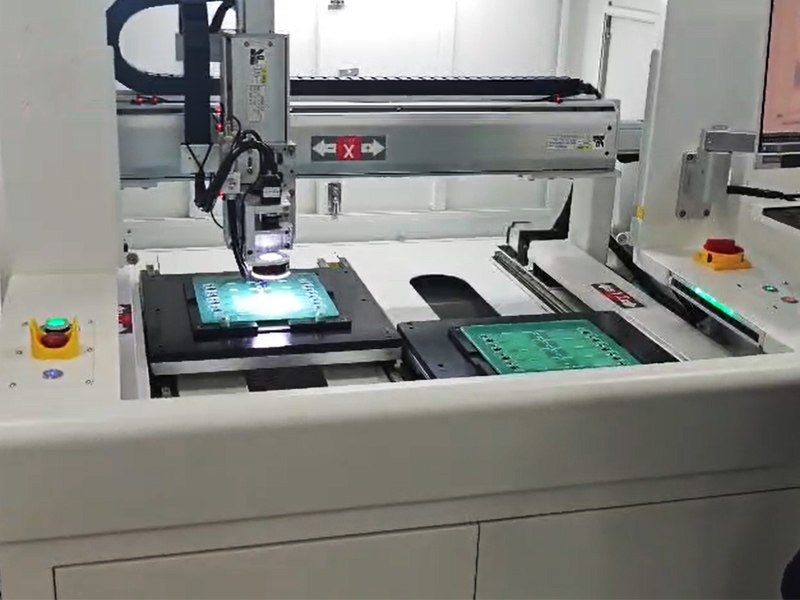
- LED and Mini LED COB Packaging—Chip-on-Board LED modules require depaneling of densely packed aluminum substrates. Router and laser depaneling achieve ±0.05mm precision, preventing edge chipping that would destroy adjacent LED dies. A typical Mini LED backlight unit contains over 10,000 LEDs per panel.
- Automotive Electronics—EV power modules, ADAS sensor boards, and BMS PCBs demand zero-stress depaneling to meet AEC-Q100 standards. Temperature cycling tests (-40°C to +125°C, 1,000 cycles) reveal micro-cracks from mechanical depaneling propagate under thermal stress.
- AI Server and HPC Motherboards—Next-gen GPU racks feature PCBs with 20–26 layers and trace widths under 50μm. PCB value per rack has surged from approximately $35,000 to $117,000. At these price points, depaneling errors are unacceptable.
- Consumer Electronics—Smartphones, wearables, and IoT devices use ultra-thin flex circuits that cannot tolerate mechanical forces. Laser depaneling processes these substrates at production line cadences.
- Industrial and Medical Equipment—High-reliability sectors require both precise depaneling and permanent traceability. Laser engraving marks each PCB with unique Data Matrix codes surviving soldering, washing, and conformal coating.
5. Expert FAQ: PCB Depaneling and Laser Engraving
Q1: What is PCB depaneling and why does it matter in 2026?
PCB depaneling is the process of separating individual circuit boards from a larger production panel after assembly. In 2026, depaneling precision has become critical because AI server and automotive-grade PCBs require near-zero stress separation to prevent micro-cracks, solder joint damage, and component failure. With global PCB output exceeding $900 billion, depaneling quality directly impacts end-product reliability and manufacturing yield rates.
Q2: What are the main types of PCB depaneling methods?
There are three primary PCB depaneling methods in 2026: V-Cut (V-Scoring) uses upper and lower circular blades—ideal for high-volume, rectangular panels. Router Depaneling employs high-speed milling spindles for irregular board shapes and precision-sensitive designs. Laser Depaneling uses UV or fiber lasers for non-contact, stress-free cutting, best for flexible circuits, ultra-thin boards, and high-density interconnect PCBs.
Q3: How does laser depaneling compare to V-Cut in cost?
Laser depaneling has higher upfront equipment cost (3-5x V-Cut), but delivers lower per-unit processing cost for high-mix, precision-critical applications. V-Cut remains most cost-effective for high-volume, standardized shapes. The ROI tipping point depends on production volume, board complexity, and quality requirements. For AI server and automotive applications where stress defects cost thousands per recall event, laser's precision premium is justified.
Q4: What role does laser engraving play in PCB manufacturing?
Laser engraving extends beyond cutting to include traceability marking—permanently etching Data Matrix codes, QR codes, serial numbers onto circuit boards. This supports IPC-1782 traceability standards, anti-counterfeiting, and automated optical inspection. In 2026, laser marking has become mandatory for automotive electronics suppliers and is rapidly adopted across consumer and industrial segments.
Q5: How do I choose the right PCB depaneling solution?
Selection depends on four factors: (1) Production volume—V-Cut for high-volume, router for mixed shapes, laser for high-mix precision. (2) Board material—FR4 works with all methods; aluminum and flex benefit from laser/router. (3) Precision requirements—components within 0.5mm of cut edge require router or laser. (4) Budget and ROI—calculate TCO including maintenance, consumables, and defect reduction savings.
Q6: Can V-Cut depaneling be used for flexible PCBs?
No. V-Cut is designed for rigid boards with pre-scored grooves. Flexible PCBs lack the rigidity for blade separation and would deform. Flex and rigid-flex circuits should use router depaneling with vacuum fixturing or—preferably—laser depaneling, which exerts no mechanical force on the substrate.
Q7: What are the 2026 trends driving depaneling innovation?
Key trends: (1) AI server PCBs with 20+ layers demanding zero-stress separation; (2) Mini LED/COB requiring micron-level precision; (3) EV electronics with stringent reliability; (4) Industry 4.0 integration—inline machines with MES connectivity and AI vision; (5) Miniaturization pushing component density, leaving tighter depaneling tolerances.
6. 2026 Outlook: The Future of Smart Depaneling
Technology convergence: Next-generation machines combine router and laser capabilities in a single platform, enabling manufacturers to select the optimal cutting method per job without equipment changes.
Inline integration: Depaneling moves from standalone workstations to fully integrated inline systems. Modern lines connect solder paste printing, pick-and-place, reflow soldering, and AOI with smart depaneling modules receiving board-specific programs from MES in real time.
Sustainability: Environmental considerations drive dust-free laser depaneling and closed-loop cooling systems reducing energy consumption by up to 35% compared to previous generations.
Explore JHIMS's latest solutions in cutting, depaneling, and laser engraving equipment—engineered for the precision demands of 2026 and beyond.


 Teams
Teams
 whatsapp
 telegram
