

How AOI SPI X-Ray Inspection Is Transforming PCB Quality in 2026
The global semiconductor industry is projected to reach $975 billion in 2026—growing at over 26% year-over-year. Yet behind every chip and circuit board lies a silent crisis: as PCB densities double and component sizes shrink below 0.4mm pitch, traditional quality control methods are failing at an alarming rate. Enter the inspection triad: AOI (Automated Optical Inspection), SPI (Solder Paste Inspection), and X-Ray (AXI)—three technologies that are collectively redefining what "zero-defect manufacturing" means in the SMT era.
The Current State of PCB Quality Control: 5 Pain Points Driving Change
Despite decades of advancement in SMT assembly, quality control remains the single largest source of manufacturing waste. According to IPC industry benchmarks, 60-70% of all SMT defects originate at the solder paste printing stage alone—before a single component is even placed. By the time a defective board reaches functional test, rework costs can exceed 10x the original cost of catching the defect at source.
The industry faces five interconnected challenges that traditional manual inspection simply cannot solve:
- Component Miniaturization: With 0201 and 01005 packages (0.4mm × 0.2mm) now mainstream in consumer electronics, the human eye—even under magnification—cannot reliably assess solder joint quality at production speeds.
- Hidden Interconnects: BGA, QFN, and flip-chip packages conceal critical solder connections beneath the component body. Optical inspection sees nothing; only X-Ray can reveal whether those hidden balls are properly collapsed and void-free.
- Inspection Fatigue: Studies demonstrate that human inspectors begin missing defects after just 15-20 minutes of continuous work. In 24/7 high-volume lines, this creates an unacceptable quality gap.
- Data Blindness: Manual inspection generates no structured data—no SPC trends, no root-cause traceability, no closed-loop feedback to the process. You know something failed, but not why or how to prevent recurrence.
- Rising Quality Standards: Automotive (IATF 16949), medical (ISO 13485), and aerospace (AS9100) standards now mandate automated inspection with full traceability, making manual methods non-compliant for regulated industries.
These pain points are not theoretical. A 2026 industry survey from the PCB manufacturing sector confirms that high-end PCB capacity for AI servers and advanced packaging is completely sold out, while low-end commodity boards face intense price competition. The message is clear: manufacturers who cannot guarantee quality at scale will be squeezed out of the market.
AOI, SPI, and X-Ray Inspection: The Technical Breakthroughs Reshaping 2026
The solution to these challenges is not a single technology but a multi-layered inspection architecture that addresses defects at each stage of the SMT process. In 2026, the integration of AI, 3D imaging, and high-speed X-Ray tomography has created a new paradigm in quality assurance—one that catches defects at the point of origin rather than downstream.
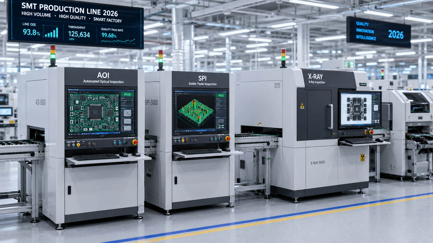
Automated Optical Inspection (AOI): The Visual Front Line
AOI systems use high-resolution cameras and multi-angle LED illumination (typically RRGB configuration) to capture detailed images of every component and solder joint post-reflow. In 2026, the dominant shift is from 2D to 3D AOI—systems that use structured light projection, laser triangulation, or Moiré interferometry to add the critical Z-axis (height) dimension.
Why does height matter? A 2D AOI sees a component as a flat 2D silhouette; it cannot distinguish between a properly seated BGA and one that is tilted 50 microns. A 3D AOI captures full topographic data—height, volume, coplanarity, and warpage—reducing false-call rates by 60-80% compared to 2D systems. Leading manufacturers including Koh Young, Omron, SAKI, PARMI, ALeader, and ZhenHuaXing now ship 3D-capable platforms as standard, and by late 2026, 3D AOI is expected to represent over 70% of global new installations.
Solder Paste Inspection (SPI): Stopping Defects Before They Happen
SPI sits at the most critical control point in the SMT line: immediately after the solder paste printer. Using 3D measurement technologies, SPI quantifies every paste deposit on every pad:
- Volume: Is there enough paste for a reliable solder joint?
- Height & Area: Does the deposit match the stencil design within tolerance?
- Offset: Is the paste aligned with the pad center?
- Bridging & Smearing: Are adjacent pads at risk of shorting?
Modern 3D SPI systems achieve measurement accuracy in the single-digit micron range and can inspect a full board in under 15 seconds. When connected via closed-loop feedback to the printer, SPI enables real-time stencil cleaning, squeegee pressure adjustment, and paste temperature control—preventing defects before a single component is placed.
X-Ray Inspection (AXI): Seeing the Invisible
X-Ray inspection is the ultimate safety net—the technology that reveals what optical and laser methods cannot. In BGA, CSP, QFN, and press-fit assemblies, the most critical solder connections are hidden from view. X-Ray passes through the component body, creating grayscale images where denser materials (solder, copper) appear darker, revealing:
- Void percentage: BGA void rates must typically stay below 25% per IPC-7095; X-Ray quantifies every void.
- Head-in-Pillow (HIP): A subtle defect where the BGA ball and solder paste make contact but fail to fully merge—invisible to AOI, catastrophic in the field.
- Insufficient ball collapse: Indicates poor reflow profile; X-Ray measures ball diameter and standoff height.
- Internal cracks & delamination: Critical for automotive and aerospace reliability.
While 2D X-Ray provides a top-down view, 3D CT (Computed Tomography) X-Ray—the gold standard—reconstructs complete volumetric models of every joint, enabling slice-by-slice inspection of multi-layer board assemblies.
Key Technical Parameters: Traditional vs. 2026 Next-Generation Inspection
| Parameter | Traditional (Pre-2023) | 2026 Next-Generation |
|---|---|---|
| AOI Imaging | 2D RGB LED, planar only | 3D structured light + multi-angle stereo |
| Minimum Detectable Defect | ~50 µm (0201 level) | ~15 µm (008004 / 01005 level) |
| False-Call Rate | 15-30% typical | 3-8% (AI-assisted classification) |
| New Product Programming | 2-6 hours (manual rule setting) | 10-30 minutes (AI auto-programming) |
| SPI Accuracy | ±15 µm height | ±3-5 µm height, ±10 µm XY |
| X-Ray Resolution | 10-15 µm per pixel (2D) | 1-5 µm per voxel (3D CT) |
| MES Integration | Limited / proprietary protocols | Full API, OPC-UA, MQTT, Industry 4.0 ready |
| Throughput | 15-25 sec/board (AOI) | 6-12 sec/board (AOI with parallel processing) |
Production Efficiency Gains: A Quantified Analysis
The financial case for integrated inspection is compelling. When manufacturers deploy a complete AOI + SPI + X-Ray chain, the measurable improvements are dramatic:
- First-pass yield improvement: Typical increase of 8-15 percentage points within the first quarter post-installation. A line producing 100,000 boards/month that moves from 92% to 99% FPY eliminates 7,000 rework cycles monthly.
- Rework cost reduction: Industry data shows that detecting a defect at SPI stage costs approximately $0.50 to correct; at post-reflow AOI, $5; at functional test, $50; and at the customer site, $500+. SPI-driven closed-loop feedback typically reduces downstream rework by 40-65%.
- Line utilization uplift: Automated inspection eliminates the bottleneck of manual visual checking. Lines with integrated AOI/SPI achieve 20-35% higher effective throughput compared to lines relying on sample-based manual inspection.
- Cpk improvement: Statistical process capability (Cpk) for critical solder paste parameters (volume, area, height) typically improves from 1.0-1.33 to 1.67-2.0+ with real-time SPI feedback, moving from "adequate" to "world-class" process control.
Cost Control and Maintenance Optimization
Beyond the headline efficiency gains, modern inspection systems deliver significant operational cost benefits:
- ROI Timeline: A typical mid-range AOI+SPI system investment ($80,000-$150,000) achieves breakeven within 8-14 months through rework reduction alone—before accounting for the value of scrap prevention and customer returns avoidance.
- Maintenance Cycle Extension: AI-powered self-diagnostic features in 2026-generation systems predict component wear (lenses, lighting modules, X-Ray tubes) and schedule maintenance during planned downtime. Unplanned inspection downtime drops by 50-70% compared to calendar-based maintenance approaches.
- Programming Labor Savings: AI auto-programming reduces new product setup from 4-6 engineering hours to under 30 minutes. For high-mix manufacturers launching 20+ new products monthly, this alone saves 80-120 engineering hours per month.
- Warranty Cost Reduction: A major EMS provider reported a 72% reduction in field returns within 18 months of deploying integrated AOI+SPI+AXI, translating to over $2 million in annual warranty cost savings.
For a detailed overview of available inspection technologies, explore the AOI SPI X-Ray Series product line, which covers the complete spectrum from entry-level 2D AOI to advanced 3D CT X-Ray systems.
Real-World Application Scenarios in 2026
The adoption of automated inspection is no longer limited to the world's largest electronics manufacturers. Across industries, 2026 is the year that AOI, SPI, and X-Ray become standard infrastructure across diverse production environments:
Automotive Electronics
Under IATF 16949 requirements, automotive Tier-1 and Tier-2 suppliers must demonstrate zero-defect capability for safety-critical assemblies (ECUs, ADAS modules, battery management systems). A typical automotive PCB contains 500-2,000 components with multiple BGAs and QFNs—making X-Ray inspection mandatory for every board, not just sample-based. AOI verifies visible joint quality, while 3D CT X-Ray validates hidden interconnects, providing the complete traceability dossier required for PPAP submissions.
Consumer Electronics
Smartphone and wearable manufacturers operate at the extremes of miniaturization and speed. With 01005 components and 0.3mm-pitch BGAs now standard, 3D AOI with AI classification has become the only viable approach to maintain defect escape rates below 50 DPM (defects per million) at production speeds exceeding 40,000 CPH (components per hour). Leading smartphone brands now specify 3D AOI as a mandatory equipment requirement in their EMS qualification checklists.
LED and Display Manufacturing
Mini-LED and Micro-LED backlight modules present unique inspection challenges: thousands of identical, densely packed dies on a single substrate, where a single dead pixel can make a display unsaleable. SPI systems adapted for LED die-attach paste inspection measure deposit uniformity across thousands of positions per board, while specialized AOI algorithms verify die placement accuracy within ±10 µm. For GOB (Glue-On-Board) LED module encapsulation, 3D AOI validates coating coverage and thickness.
Medical Device Electronics
Implantable and life-sustaining medical electronics are governed by ISO 13485 and FDA 21 CFR Part 820, which require complete device history records (DHR) including inspection data for every unit. Integrated inspection systems with full MES connectivity automatically generate the required traceability packages—from SPI paste deposit records through post-reflow AOI images to X-Ray void analysis—reducing documentation labor by over 80% while ensuring audit-readiness.
Industrial and Power Electronics
High-current power modules, IGBT assemblies, and industrial motor drives use heavy copper boards (4-10 oz) and large-form components that generate significant thermal stress. X-Ray inspection is essential for detecting voids in thick solder joints that can create hot spots and lead to premature failure. 2D X-Ray with automated void calculation (reporting void percentage per IPC-7095) has become the standard for power electronics quality release.
Expert FAQ: AOI, SPI, and X-Ray Inspection in 2026
Q1: What is the fundamental difference between AOI, SPI, and X-Ray inspection?
A: Each targets a different stage and defect type. SPI inspects solder paste deposits immediately after printing—measuring volume, height, area, and alignment before components are placed. AOI inspects visible components and solder joints after placement and reflow, using cameras and multi-angle lighting to detect missing parts, bridges, tombstones, and polarity errors. X-Ray (AXI) inspects hidden solder connections—BGA balls, QFN thermal pads, and press-fit pins—that optical methods cannot access. They are complementary, not alternatives: a complete quality strategy uses all three.
Q2: Why is 3D AOI replacing 2D AOI in 2026?
A: 2D AOI analyzes flat images; it cannot measure height, volume, or coplanarity. This fundamental limitation means it struggles with lifted components, insufficient solder (where only height reveals the problem), and components that match the board color. 3D AOI adds the Z-axis dimension using structured light or laser triangulation, enabling true volumetric inspection. The result: 60-80% lower false-call rates and the ability to detect defect types that 2D systems simply miss. With 3D system costs now within 20-30% of 2D equivalents, the business case for staying with 2D has largely evaporated.
Q3: How does AI improve AOI defect detection accuracy?
A: Traditional AOI uses rule-based algorithms—engineers manually define thresholds for brightness, color, and shape. This approach generates high false-call rates because it cannot distinguish between a genuine defect and acceptable process variation. AI-powered AOI uses deep learning models (such as YOLO11 and custom CNNs) trained on thousands of verified good and defective images. The AI learns to recognize defect patterns the way an experienced human inspector would—but faster and consistently. Key benefits include auto-programming in minutes instead of hours, 50-80% false-call reduction, and continuous accuracy improvement as the system processes more boards.
Q4: What types of defects can X-Ray detect that AOI cannot?
A: X-Ray is essential for defects hidden beneath component bodies. These include: BGA solder voids (quantified as a percentage per IPC-7095, typically requiring <25%), Head-in-Pillow (HIP) defects where the ball and paste make contact but fail to fully merge, insufficient ball collapse indicating poor reflow, internal cracks and delamination in multi-layer boards, and QFN thermal pad solder coverage. For any assembly containing BGAs, CSPs, or QFNs, X-Ray inspection is not optional—it is the only technology that can verify the integrity of hidden interconnects.
Q5: How do I determine the right inspection configuration for my production line?
A: The decision framework depends on three factors: production volume, product complexity, and industry regulation. Low-volume / prototype lines benefit from offline AOI for cost-effective quality assurance. Medium-volume lines (100-1,000 boards/day) should deploy online AOI + SPI to catch the majority of defects inline. High-volume or regulated lines (>1,000 boards/day, especially automotive, medical, or aerospace) need the full AOI + SPI + X-Ray chain with 3D capability. The investment logic is straightforward: the cost of one field failure in a safety-critical application can exceed the entire inspection capital expenditure by orders of magnitude.
Q6: What ROI can I expect from investing in automated inspection?
A: A typical AOI+SPI system investment ($80K-$150K) achieves payback in 8-14 months through rework reduction alone. Key ROI drivers include: rework cost avoidance (each defect caught at SPI costs ~$0.50 to fix vs. $500+ at the customer site), scrap reduction (preventing entire boards from being scrapped due to undetected defects), programming labor savings (AI auto-programming cuts setup from hours to minutes), warranty cost reduction (some EMS providers report 70%+ reductions in field returns), and increased line utilization (20-35% throughput improvement by eliminating manual inspection bottlenecks).
Q7: What are the key trends shaping inspection technology beyond 2026?
A: Three major trends will define the next generation: AI self-learning systems that continuously improve accuracy by observing operator classification decisions; multi-modal fusion inspection combining optical, thermal, and X-Ray data into a unified defect assessment; and digital twin integration where virtual inspection cells simulate new product introductions before physical deployment. Additionally, edge AI processing is enabling real-time defect classification without cloud dependency, while OPC-UA and MQTT protocols are standardizing MES integration across vendor platforms.
2026 and Beyond: Building a Future-Proof Quality Strategy
The trends shaping 2026 are unmistakable: PCB complexity is accelerating, quality standards are tightening, and the cost of failure is rising exponentially. The manufacturers who thrive in this environment will be those who treat inspection not as a cost center but as a strategic capability—one that protects revenue, builds customer trust, and enables entry into high-value regulated markets.
The roadmap is clear:
- Start at the source with 3D SPI to eliminate the 60-70% of defects that originate at paste printing.
- Cover the visible spectrum with 3D AI-powered AOI that catches surface-level defects with minimal false calls.
- Reveal the hidden with X-Ray inspection for BGA, QFN, and advanced packaging assemblies where optical methods reach their limit.
- Connect everything through MES integration that transforms inspection data into real-time process control, not just pass/fail records.
For manufacturers evaluating their next quality investment, JHIMS offers a comprehensive portfolio spanning the full inspection chain—from entry-level AOI and SPI systems to advanced 3D X-Ray CT solutions. Explore the AOI SPI X-Ray Series to find the configuration that matches your production requirements, or contact our engineering team for a tailored consultation.


 Teams
Teams
 whatsapp
 telegram
